dScope Series III Architecture Guide
DIGITAL INPUT AND CARRIER CIRCUITS
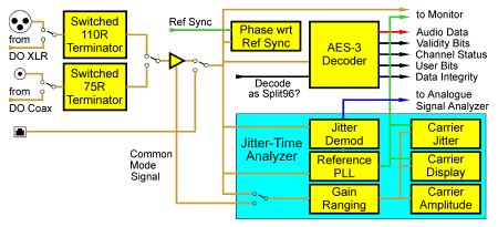
The figure above illustrates the functionality of the Digital Input and Carrier circuits. The settings and Results for these sections are accessed through the Digital Inputs dialogue box:
and the Digital Input Carrier dialogue box.

The digital audio input is selected from the XLR, BNC or TOSLINK front-panel DI connectors, or the XLR or BNC Digital Outputs can be looped back. The XLR and BNC options may be terminated appropriately if required. In 'loop-through' modes, the termination can be lifted to allow the dScope to analyze 'in-line'.
The selected input is routed to the AES3 decoder, where its various data components are distributed for audio and status analysis. It is also compared with the Digital Output reference for the 'Phase wrt Ref Sync' Result. The selected input is also fed to the monitor section (for carrier and sync-pulse output modes) and to the JTA (Jitter Time Analyzer). The settings of the incoming channel status data are displayed in a simplified form (below)

and an advanced form (below)

The JTA is a sophisticated processing block which performs carrier timing and amplitude measurements, and can be used to plot a Carrier Display or eye-diagram (below)

Note that the JTA also demodulates any jitter present on the Digital Input, and this signal can be switched to the Analogue Input of the dScope's Signal Analyzer for time-domain and spectral (FFT) analysis. This selection is made in the Analogue Inputs dialogue box.


